Jan 2025 – Feb 2025
EELast edited
Quantization-Limited SNR on a 12-bit Multi-ADC Pipeline
Built a measurement system for digitising analog signals using a Raspberry Pi 3B with external MCP3201 12-bit ADCs and an op-amp low-pass filter front end. The system was evaluated through frequency-domain analysis, time-series inspection, and signal-to-noise ratio (SNR) calculations.
Verification confirmed correct waveform and amplitude reproduction, but identified a systematic DC offset visible in every FFT. Measured SNR at 1 kHz, 2 kHz, and 10 kHz was 55.22, 55.14, and 55.18 dB respectively, essentially flat across frequency, but ~19 dB below the 74 dB ideal-quantisation bound for a 12-bit converter.
The gap is consistent with quantisation noise in non-full-scale regions, power-supply interference, a lower-than-designed actual cutoff in the analog low-pass filter, and reference-voltage instability. Improvements identified for a follow-up: better EMI shielding, a low-noise reference, a more precise filter implementation, and post-hoc calibration of the systematic offset.
Affiliation
NTNU
Partners
Report
- Lab report
Keywords
- Digital Signal Processing (DSP)
- Quantization
- Noise Analysis
- Fast Fourier Transform (FFT)
- C
- Python
- Raspberry Pi
- MCP3201 ADC
▸ Deepdive
Introduction
This project is the measurement front-end for a radar/microphone pipeline built around a Raspberry Pi 3B+ and five external Microchip MCP3201 12-bit ADCs sampled in parallel over a shared SPI bus. The Pi has no native analog inputs, so the entire signal-acquisition chain hangs off SPI: a single DMA-driven clock and chip-select line is broadcast to all five ADCs, while each device’s MISO returns on its own GPIO, letting the host capture five simultaneous channels per SPI transaction. The lab was scoped around verifying that the pipeline actually delivers the precision its datasheet promises, quantization-limited SNR at 12 bits is , and the question is how close a real, breadboard-mounted, supply-noisy implementation gets to that bound.
Problem Definition
Each ADC samples a continuous voltage at rate and emits a discrete code with . The Nyquist–Shannon condition fixes the upper end of the bandwidth that can be captured without aliasing,
and the resolution of each code is the LSB step
so the worst-case quantization noise amplitude is
For a full-scale sinusoidal input, the theoretical SNR of an ideal -bit ADC is the standard result
which sets the headline target. The empirical SNR is computed from the measured spectrum as
with the energy in the input tone’s bin (and its image), and the integrated energy across the rest of the spectrum (DC bin excluded, since the DC offset is a deterministic bias rather than noise). The lab’s job is to quantify the gap between and the realized across three input frequencies and to attribute that gap to the dominant noise sources in the chain.
Approach
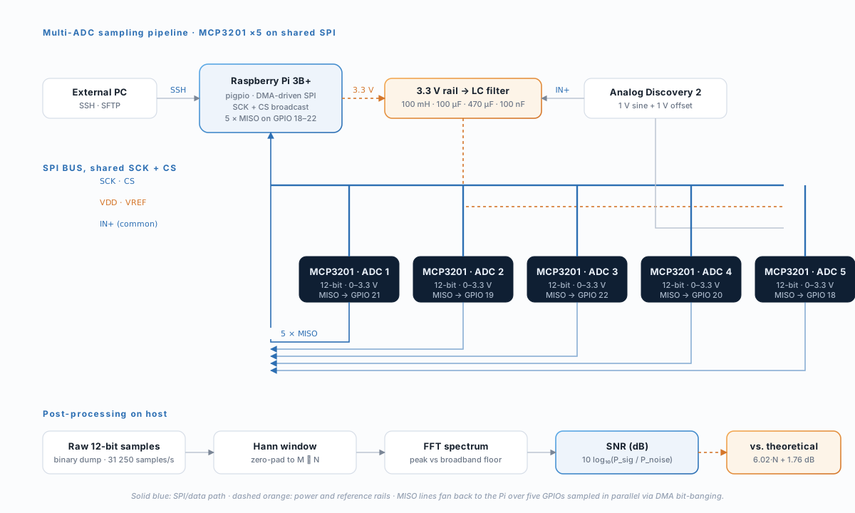
The pipeline decomposes into four stages: a Raspberry Pi host configured for headless data acquisition, a multi-ADC SPI fan-out with a shared clock and per-channel MISO, an LC supply filter on the 3.3 V rail, and a host-side spectral-analysis pipeline that converts raw codes into SNR figures.
Raspberry Pi Host and SPI Fan-Out
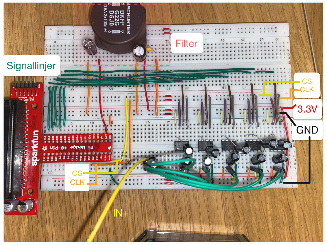
The Pi is flashed with 32-bit Raspberry Pi OS via the Imager (with SSH, hostname, and Wi-Fi pre-configured), reached over SSH for control and SFTP for pulling sample dumps. All five MCP3201s share the SCK and CS lines and differ only in the GPIO their MISO is wired to (GPIO 18, 19, 20, 21, 22). A traditional SPI master would drive each device through its own CS, but the MCP3201 starts a fresh conversion on every CS falling edge regardless of MISO ownership, so a single CS pulse drives all five conversions simultaneously and the host reads the five MISO bits in lock-step. The C client uses pigpio’s rawWaveAddSPI interface, which DMA-bit-bangs the SPI transaction so the bit timings are guaranteed to within roughly and the CPU is left free for buffer management. Sample rate is set to , giving .
LC Supply Filter
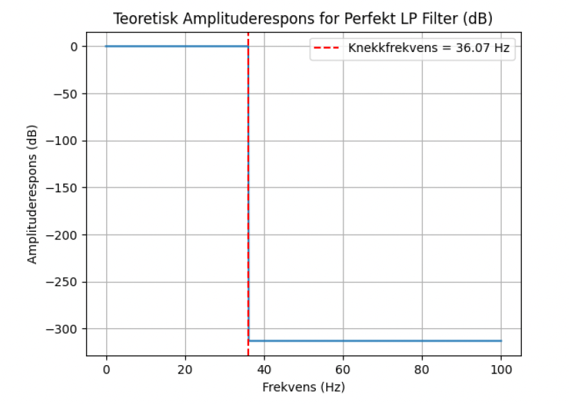
ADC resolution is only as good as the stability of (per the LSB equation above), so the 3.3 V rail is filtered before it reaches VDD and VREF. A second-order LC topology with a inductor and a capacitor stack has transfer function
and at the point , which solves to
with the nominal component values. Each ADC additionally carries two decoupling capacitors (one between VREF and IN−, one between VDD and VSS) to suppress the high-frequency switching that the SPI clock and Pi-side DC-DC injects into the rail.
Spectral Analysis and SNR
Each captured channel is windowed with a Hann window
which is a reasonable default between main-lobe width and side-lobe leakage; Hamming and Blackman were both available but Hann gave the cleanest peak/floor separation for sinusoidal test tones. The windowed sequence is zero-padded from to samples,
and the DFT is taken on the padded length,
Padding does not add information but refines the frequency-axis step, which sharpens the visual location of the peak without changing the underlying energy spectrum. The SNR formula above is then evaluated by taking as the energy in the bins at and as the energy in every other bin except DC.
Experimental Verification
A 12 V sinusoid with amplitude and DC offset (so the signal lives in , comfortably inside the ADC range) is generated by an Analog Discovery 2 (AD2) and fanned out onto a common IN+ line that all five ADCs share. The same AD2 in impedance-measurement mode is used to characterise the supply filter’s inductor over to .
Results
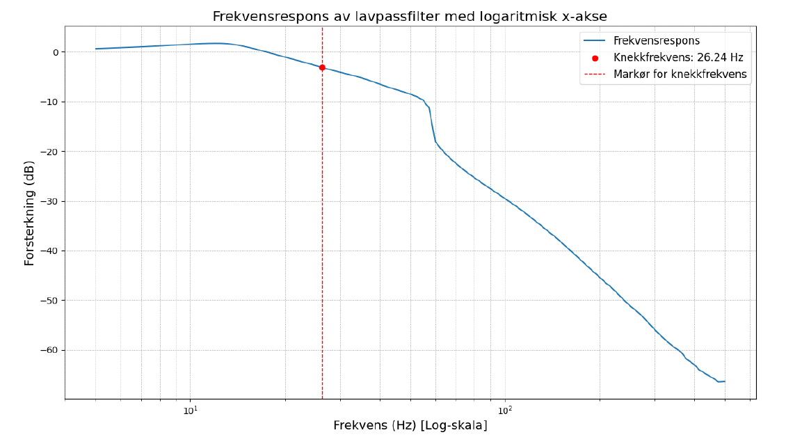
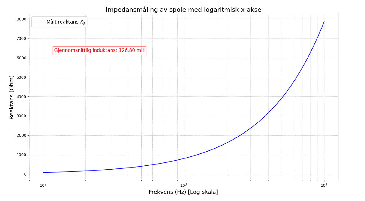
The LC filter’s measured frequency response, swept with the AD2, shows the knee at rather than the predicted . Impedance-measuring the inductor across the same sweep gives an averaged inductance of versus the nominal , which alone shifts the theoretical knee to and explains the bulk of the discrepancy, the residual shift is attributable to capacitor tolerance, the inductor’s ESR/DCR, and parasitic effects on the breadboard. A small unexpected secondary knee around is consistent with mains-frequency pickup or a resonance in the breadboard layout.
The ADC chain was driven with single-tone sinusoids at three frequencies and the SNR computed channel-by-channel. The realized SNR sits about below the 12-bit quantization bound and is essentially flat across the three test frequencies, which is consistent with broadband noise (quantization, supply ripple, and EMI pickup) dominating over any frequency-dependent loss in the analog front-end.
| Input tone | Empirical SNR | Theoretical | Gap |
|---|---|---|---|
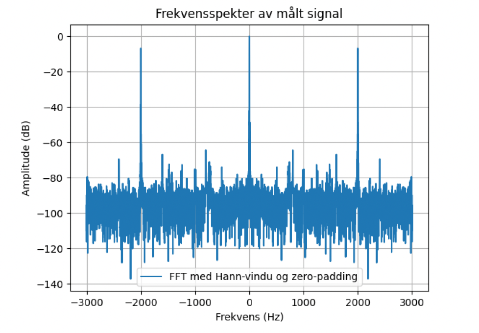
The ceiling is itself the quantization-limited SNR: the LSB-floor noise of an ideal 12-bit quantizer, with no other error source present. Hitting it requires that every other contributor, supply ripple, reference drift, EMI pickup, clock jitter, breadboard parasitics, is at least below the quantization floor. The observed is therefore not a quantization-noise problem in any direct sense; quantization sets the optimistic ceiling, and the gap is entirely additive noise on top of that ceiling. The frequency-flatness of the gap across , , and is consistent with this: quantization noise is white in expectation, and so is broadband supply/EMI noise, so neither has a fingerprint that would single it out from the others without injecting a known disturbance and measuring the SNR delta.
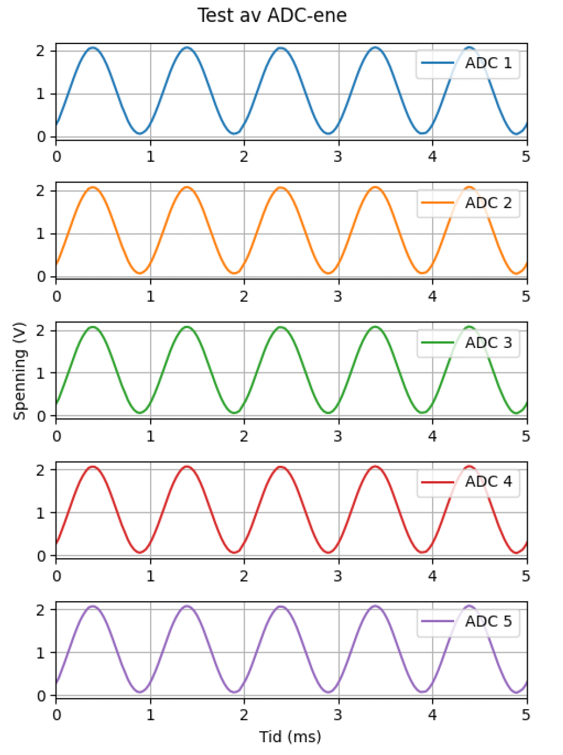
Time-domain plots of all five channels for the -amplitude -offset test tone show identical waveforms with the correct frequency and shape, but with a systematic offset: the peaks sit slightly above and the troughs slightly above , indicating a small, channel-independent bias on the measured DC level. Because the bias is identical across all five ADCs, it is a property of the measurement chain (reference, input impedance, breadboard drop) rather than of any individual MCP3201.
Future Work
The gap between empirical and quantization-limited SNR is the headline number to attack. Three classes of fix change the cost/benefit calculation differently. First, the analog front-end is currently a breadboard with long jumper wires and shared rails, which makes it a near-perfect aerial for EMI from the bench environment and the Pi’s own switching regulators; lifting the design onto a soldered PCB with a continuous ground pour, short trace runs, and shielded analog islands is the single largest available improvement and would also resolve the unexplained knee in the filter response. Second, the LC filter as built has a real inductance above nominal, which both shifts the cutoff and adds DCR-driven attenuation in the passband, replacing the inductor with a tighter-tolerance part (or characterising the actual before laying out the filter) removes a contributor to in-band signal loss that directly drags down in the SNR ratio. Third, a more stable voltage reference (a dedicated or precision reference rather than the Pi’s 3.3 V rail) tightens and therefore tightens the LSB, which removes a multiplicative noise term that the current rail leaves on the table.
The systematic offset visible in every ADC time series is a separate problem and a much cheaper one to solve. Because the offset is identical across channels and stable across runs, it can be measured once at calibration time (drive a known into IN+, read all five codes, store the per-channel offset ) and subtracted in software during post-processing. Texas Instruments publishes a standard recipe for this kind of two-point ADC calibration; folding it into the existing Python pipeline is a few lines of code and removes a bias that currently has to be accounted for downstream every time the system is used.
A more fundamental redesign for the next iteration is to replace the bit-banged SPI master with the Pi’s native hardware SPI peripheral. The DMA-bit-banged path was chosen because it lets five independent MISO lines be sampled in lock-step on a controller that has only one hardware SPI peripheral, but it costs a non-trivial amount of CPU bandwidth in rawWaveAddSPI setup and limits the maximum sustainable sample rate well below what the MCP3201 datasheet permits ( at , faster at ). Moving to a multi-channel ADC (or to a Pi 4/5 with multiple hardware SPIs) lifts that ceiling and pushes the project toward the radar/microphone sample rates the eventual application needs.